Bare Metal and Registers with NXP FRDM MCX A346
Introduction
This article demonstrates a (partially pure) bare metal blinky project for the FRDM MCX A346 of NXP. The purpose is to show that embedded programming is basically manipulating the data of various kinds of registers. This may help build an intuition about what you're actually doing with the hardware as an embedded programmer on a detailed level.
I will discuss these different kinds of registers and how we are manipulating these registers using our code. I'll will also demonstrate some register views of the MCUXpresso IDE. I will also deliberately cause and discuss a bus fault so in the future, if you run into a bus fault, you can find the cause of a bus fault more quickly.
Prerequisites
- MCUXpresso IDE installed
- NXP FRDM MCX A346 board
- Documentation, especially the MCXAP144M240F60RM Reference Manual (rev 4) (download link)
Registers
If you search online for what registers are in the context of computer science, you'll find all different kinds of explanations and various distinctions between types of registers. This can be very confusing. However, these explanations are all useful within their own context.
So the explanation I will give here is just one example of a description of registers. I have chosen the distinctions I make, because I think they are relevant in the context of this project. I hope these explanations will help shape your mental model about the interaction between the software and the hardware of a microcontroller. The explanation and distinctions I make should not be treated as exhaustive or definitive. Please keep in mind that in a different context, a different mental model could be more suitable for thinking about registers.
What are registers? Physical vs. logical
In the context of computer science, the term "register" is a broad term. Physically, some registers, like status registers, are flip-flops or latches, or groups of flip-flops or latches. A flip-flop is a group of transistors which generates an electric output (i.e. 1.2V or 0V) based on inputs (i.e. 1.2V or 0V). Since there's a whole variety of types and designs of flip-flops, details about the physical nature of flip-flops and registers vary.
Other registers, like action registers, physically are groups transistors forming logic gates, which perform write operations through a brief electric pulse, which in turn triggers other physical logic. Eventually this can lead to an LED being lit. These action registers are not physically flip-flops and do not store values.
From a logical perspective a status register is a bit or a group of bits, representing logic 0 or 1. The output can be collected by a data bus.
Flip-flops are a physical part of the silicon and "not visible" to the software. From a software perspective registers can be memory mapped, though this is not always the case.
An example of a memory mapped register is the GPIO register. The Port Data Direction Register (PDDR) stores the direction of a GPIO pin (input or output). The Reference Manual of the FRDM MCX A346 tells us the registers for GPIO3 have the address 4010_5000h and the PDDR registers have an offset 54h, so 4010_5054h.
If we want to set the direction of pin P3_18 (the onboard red LED) to output, we can write a line of code like this:
*(volatile uint32_t*)(0x40105054) |= (1U << 18);
This "address" can also be thought of as a code or bus route label which is decoded by a bus matrix so it knows to which peripheral the data has to be sent. Additional steps include an APB‑bridge, a peripheral address decoder and a register write to a flip-flop. Physically, the flip‑flops are located inside the peripheral block, often near the I/O pads.
Status registers vs. action registers
I make the distinction between status registers on one hand and action registers on the other, for reasons of debugging.
Status registers can be set to value and they retain this value until they are changed. Action registers do not store a value. They trigger an action. This means you won't be able to debug these registers by reading their value using PRINTF(), because no data is stored. So PRINTF() commands which read the value of an action register will always read zero. Examples of action registers are MRCC0->MRCC_GLB_CC0_SET (AHB Clock Configuration field) and GPIO3->PTOR (Port Toggle Output).
Status registers on the other hand can be read and debugged using PRINTF(). Examples of status registers are MRCC0->MRCC_GLB_CC1 (AHB Clock Control; determines whether the clock for the respective peripheral is active), SYSCON->CLKUNLOCK (controls clock configuration registers access), PORT3->PCR[18] (Pin Control Register with configuration fields such as Input Buffer Enable, Pin Multiplex (MUX) Control, Pull Enable, Pull Select, etc.) and GPIO3->PDDR (Port Data Direction; GPIO input or output).
Core registers vs. peripheral registers
Obviously, core registers are related to the CPU core, whereas peripheral registers are related to peripherals. Core registers store a very small amount of temporary working data used by the CPU while executing instructions. Because they are physically part of the CPU datapath, they are faster than cache or any other form of memory.
Examples of core registers are the stack pointer, program counter and scratch registers (ARM: "used to hold an intermediate value during a calculation").
Peripheral registers represent the configuration, status, and command interface of peripherals such as GPIO, ADC, DMA, etc. They physically reside inside the hardware block of each peripheral, not in the CPU core.
Again, I make this distinction for debugging purposes. In the next paragraph, I'll discuss the Registers View and the Peripherals+ View of the MCUXpresso IDE. The Registers View shows the core registers, while the Peripherals+ View shows the peripheral registers. So the purpose of the distinction I make is to help you look at the right place when debugging.
Peripherals+ View
To open the Peripherals+ View in the MCUXpresso IDE, in the taskbar: Window > Show View > Peripherals+, or Window > Show View > Other... > MCUXpresso IDE > Peripherals+.
The Peripherals+ View is an empty grid if you're not debugging. Once you Build and Debug, the grid will be filled with a list of peripherals.
Let's test this by copying the code below into a new C project. Build and Debug and open the Peripherals+ View. Expand GPIO3 > expand PDDR, scroll down to PDD18.
Place the cursor at the beginning of this line:
GPIO3->PDDR |= (1U << 18);
Right click and click Run to Line. You'll notice the Value fields fill up. PDD18 has a value of pdd0.
Click the Step Into button.

Inside the Peripherals+ View the value of PDD18 should now have changed into pdd1.
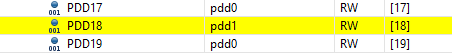
So this is another way of debugging the status registers of peripherals.
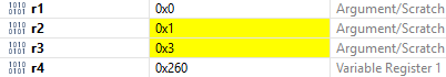
Registers View
The Registers View is probably already available next to the Project Explorer, but if that isn't the case for you: Window > Show View > Other... > Debug > Registers.
The Registers View is empty if you're not debugging. Once you Build and Debug, the grid will be filled with a list of peripherals.
Build and Debug and open the Registers View.
Place the cursor at the beginning of this line:
int a = 1;
Right click and click Run to Line.
Click the Step Into button a couple of times and you'll see the values of one or more of registers r0 to r3 change and hold the hex value of 1 (0x1), 2 (0x2), 3 (0x3) and 1 again.
Debugging a bus fault
We're going to deliberately cause a bus fault by commenting out this line:
RESET_ReleasePeripheralReset(kPORT3_RST_SHIFT_RSTn);
If we Build, Debug and Resume debug session, a bus fault occurs.
Although we already know the cause in this experiment, it is important to understand what is happening.
A peripheral has two independent control mechanisms:
- Clock gating, which determines whether the peripheral receives a clock
- Reset, which forces all flip flops in the peripheral into their default state
When a peripheral is held in reset, its registers etc. are forced into a known, safe default state. This is implemented physically by asserting the peripheral's reset line. As long as reset is asserted, the peripheral ignores all register writes.
To configure a peripheral, its reset line must be released, so the flip flops can operate normally and the peripheral can respond to register writes.
If we skip the reset release step, the peripheral remains in its default state and configuration writes have no effect. In some cases (depending on clock gating and initialization order) this can also lead to a bus fault when the peripheral is accessed before it is fully enabled.
Possible debugging steps
In the Faults View you'll probably see:
BFARVALID (7) Busfault Address Register (BFAR) valid flag
PRECISERR (1) Precise data bus error
This means we know the exact register which causes the bus fault. We can check this register by looking at the value of BFAR Fault Status Register: in this case 0x400BF0C8.
If we take a look at the Peripheral+ View and sort by Location, you can look up 0x400BF000, which is PORT3. If you expand PORT3 you'll notice red text and empty Value fields. This means that the registers exist and can be found, but for some reason, the registers cannot be read. Location 0x400BF0C8 maps to PCR18, so the Pin Control Register 18 of PORT3 cannot be read.
Generally this means that this peripheral is not active. This usually happens when the peripheral is still held in reset or its clock is disabled. In our case we know this happens because the peripheral is still held in reset, because we haven't released the reset line of PORT3.
Hopefully, this will help you in the future if you run into this type of bus fault: either the clock is disabled or the peripheral is held in reset.
As a reminder though, correctly using the Pins Tool is probably the best way to prevent bus faults and to configure pins, clocks and release.
Code
#include <stdio.h>
#include "board.h"
#include "peripherals.h"
#include "pin_mux.h"
#include "clock_config.h"
#include "fsl_debug_console.h"
#include "fsl_port.h"

int main(void) {

    BOARD_InitBootPins();
    BOARD_InitBootClocks();
    BOARD_InitBootPeripherals();
#ifndef BOARD_INIT_DEBUG_CONSOLE_PERIPHERAL
    BOARD_InitDebugConsole();
#endif

    int a = 1;
    int b = 2;
    int c = a + b;

    //CLOCK_EnableClock(kCLOCK_GatePORT3);
    uint32_t cc = MRCC0->MRCC_GLB_CC1;
    PRINTF("MRCC CC PORT3 = 0x%08X\r\n", cc);
    uint32_t reg_offset         = CLK_GATE_REG_OFFSET(kCLOCK_GatePORT3);
    uint32_t bit_shift          = CLK_GATE_BIT_SHIFT(kCLOCK_GatePORT3);
    volatile uint32_t *pClkCtrl = (volatile uint32_t *)((uint32_t)(&(MRCC0->MRCC_GLB_CC0_SET)) + reg_offset);
    PRINTF("CLKUNLOCK = 0x%08X\r\n", SYSCON->CLKUNLOCK);
    SYSCON->CLKUNLOCK &= ~SYSCON_CLKUNLOCK_UNLOCK_MASK;
    PRINTF("CLKUNLOCK = 0x%08X\r\n", SYSCON->CLKUNLOCK);
    *pClkCtrl = (1UL << bit_shift);
    SYSCON->CLKUNLOCK |= SYSCON_CLKUNLOCK_UNLOCK_MASK;
    PRINTF("CLKUNLOCK = 0x%08X\r\n", SYSCON->CLKUNLOCK);
    cc = MRCC0->MRCC_GLB_CC1;
    PRINTF("MRCC CC PORT3 = 0x%08X\r\n", cc);

    RESET_ReleasePeripheralReset(kGPIO3_RST_SHIFT_RSTn);
    RESET_ReleasePeripheralReset(kPORT3_RST_SHIFT_RSTn);

    //PORT_SetPinMux(PORT3, 18U, 0U);
    PORT3->PCR[18] = ((PORT3->PCR[18] & (~(PORT_PCR_MUX_MASK))) | PORT_PCR_MUX(0U));
    PRINTF("PORT3 PCR18 = 0x%08X\r\n", PORT3->PCR[18]);

    PRINTF("GPIO3 PDDR = 0x%08X\r\n", GPIO3->PDDR);
    //*(volatile uint32_t*)(0x40105054) |= (1U << 18);
    GPIO3->PDDR |= (1U << 18);
    PRINTF("GPIO3 PDDR = 0x%08X\r\n", GPIO3->PDDR);

    while(1)
    {
        GPIO3->PTOR = (1U << 18);
        SDK_DelayAtLeastUs(500000, CLOCK_GetFreq(kCLOCK_CoreSysClk));
    }
    return 0 ;
}
Conclusion
You have learned what registers are, what different kinds of registers are and why that matters for debugging.
You have learned how to Peripheral+ View and the Registers View of the MCUXpresso IDE.
You have also learned what generally causes a bus fault.