ADC interrupt Demo with NXP FRDM MCX A346
Introduction
This project demonstrates how to adapt the lpadc_interrupt SDK example provided by NXP in the MCUXpresso IDE so it can serve as a comprehensible foundation for your own bread application. It builds on my previous article about the lpadc_polling example, again using a light-dependent resistor (LDR) to generate analog signals for the Analog-to-Digital Converter (ADC).
In that earlier article, I explained several deliberate design choices and showed how to navigate the IDE. I also discussed the importance of using interrupts instead of polling for time-critical events in my article on GPIO interrupts. If you haven't read those yet, I recommend doing so first, as they provide useful context for the concepts explored here.
Beyond demonstrating the lpadc_interrupt example in a breadboard setup, this article also takes a closer look at the FIFO (First In, First Out) mechanism where ADC conversion results are temporarily stored. Finally, we begin exploring how to read the Reference Manual effectively and how to connect its hardware descriptions to the SDK driver functions you use in code.
Prerequisites
- MCUXpresso IDE installed
- NXP FRDM MCX A346 board
- Breadboard, 3 male jumper wires, 1 LDR, 1 10 kΩ resistor
- Documentation, especially the MCXAP144M240F60RM Reference Manual (rev 4) (download link)
- Familiarity with the Pins Tool (see previous article)
FIFO (First In First Out)
The Reference Manual (section 46.3.8 Result FIFO operation) says:
"The ADC includes 1 8-entry FIFO in which the result of ADC conversions are stored. [...] Each FIFO can be emptied by successive reads of RESFIFOa."
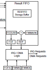
A FIFO is a queuing mechanism in which the first incoming data point is also processed first. In our case, these are the ADC conversion values. The RESFIFO (Result FIFO) is not a software buffer but a small piece of dedicated hardware memory within the LPADC peripheral itself (see Figure 207, ADC Block Diagram in the Reference Manual).
Watermark and FCTRL
The Reference Manual continues:
"A programmable watermark threshold supports configurable notification of data availability. When FCTRLa[FCOUNT] is greater than FCTRLa[FWMARK], the associated RDY flag is asserted."
This means you can set a watermark threshold (0-7). As soon as the number of stored results (FCOUNT) exceeds that threshold (FWMARK), the hardware sets the RDY flag. In our example, we choose a watermark of 2, so that 3 ADC conversions are stored before the RDY flag is activated. Think of water in a reservoir: the watermark determines how high it can rise before a signal is received.
The register that controls this is the FCTRL (FIFO Control Register). This determines the configuration and behavior of the FIFO engine. In the SDK, you can see this in fsl_lpadc.c:
base->FCTRL = ADC_FCTRL_FWMARK(config->FIFOWatermark);This is done in LPADC_Init(). In your own code, you can set this via:
mLpadcConfigStruct.FIFOWatermark = 2;LPADC_Init() receives a pointer to the entire mLpadcConfigStruct configuration structure. This allows the driver to read all LPADC settings (including the FIFO watermark) and write them into the corresponding hardware registers during initialization.
loopCount
Earlier the Reference Manual (section 46.3.4 Trigger detect and command execution) says:
"When a conversion is completed (including hardware averaging when CMDHa[AVGS] is non-zero), the result is placed in a RESFIFO buffer. When an ADC command selects looping (when CMDHa[LOOP] is non-zero) a command stores multiple conversion results to the FIFO during execution of that command."
In our example, we configured a FIFO watermark of 2, which means the RDY flag is only asserted when more than 2 results are present in the FIFO. In other words, the interrupt will only fire once 3 conversion results have been stored.
If the ADC command does not select looping, the command produces only one conversion result. That single result is placed in the FIFO, but because the FIFO never exceeds the watermark, the RDY flag is never asserted. As a consequence, the interrupt never fires and the program appears to "hang".
This means the command must be configured to generate enough conversions to exceed the watermark. The number of conversions produced by a command is:
number of conversions = loopCount + 1
Since we need 3 conversions, we configure:
mLpadcCommandConfigStruct.loopCount = 2;
This ensures the FIFO receives three results, the RDY flag becomes active, and the watermark interrupt is triggered as intended.
RDY-flag and interrupt enable
The SDK defines the RDY flag as follows:
kLPADC_ResultFIFO0ReadyFlag = ADC_STAT_RDY0_MASK,
/*!< Indicates when the number of valid datawords in FIFO0 is greater than the watermark level. */
In your IRQ handler, check this flag:
void DEMO_LPADC_IRQ_HANDLER_FUNC(void)
{
    if (kLPADC_ResultFIFO0ReadyFlag)
    {
        ...
    }
}
The Reference Manual further states:
"When IE[FWMIEx] is set, a watermark interrupt request is issued."
The FWMIEx bit in the IE register (Interrupt Enable) determines whether the FIFO watermark interrupt is active. You can think of the IE register as a row of switches: each bit enables or disables a specific interrupt source. FWMIEx stands for FIFO WaterMark Interrupt Enable (x = FIFO number). If this bit is set to 1, the hardware says, "When the FIFO watermark is reached, send an interrupt to the NVIC."
In the SDK you can see this in fsl_lpadc.h:
kLPADC_FIFO0WatermarkInterruptEnable = ADC_IE_FWMIE0_MASK,
    /*!< Configures ADC to generate watermark interrupt requests
         when RDY0 flag is asserted. */
The interrupt is enabled with the following line:
LPADC_EnableInterrupts(DEMO_LPADC_BASE, kLPADC_FIFO0WatermarkInterruptEnable);
This configures the LPADC to generate an interrupt when the FIFO0 watermark condition is met (i.e., when the number of stored results exceeds the configured watermark). Without this line, the RDY flag would still be asserted internally, but the interrupt controller would never be notified.
Hardware-software connection
If you refer to Figure 207 from the Reference Manual, you can see the flow:
- The ADC writes results to the RESFIFO Storage Buffer.
- FCOUNT increments with each new value.
- As soon as FCOUNT > FWMARK, the RDY flag is set.
- Because you enabled FWMIE, the hardware generates an interrupt.
- The NVIC calls your IRQ handler, where you read the RDY flag and process the data.
Everything up to and including step 4 is done entirely in hardware; step 5 is where your software takes control.
Code
First, configure the input pin (ADC1_A12) the same way as in the previous article, using the Pins Tool.
In app.h (in your project folder > board) change the value "8U" into "12U". This "12" is the 12 in "ADC1_A12".
So instead of:
#define DEMO_LPADC_USER_CHANNEL 8Uyou should have:
#define DEMO_LPADC_USER_CHANNEL 12UBelow follows the code for your version of lpadc_interrupt.c. It is still mainly the lpadc_interrupt SDK example, but adapted to the situation where three samples are stored in the FIFO before an interrupt is triggered.
/*
 * Copyright (c) 2016, Freescale Semiconductor, Inc.
 * Copyright 2016-2022, 2024-2025 NXP
 * All rights reserved.
 *
 *
 * SPDX-License-Identifier: BSD-3-Clause
 */

#include "fsl_debug_console.h"
#include "board.h"
#include "app.h"
#include "fsl_lpadc.h"

/*******************************************************************************
 * Definitions
 ******************************************************************************/

/*******************************************************************************
 * Prototypes
 ******************************************************************************/

/*******************************************************************************
 * Variables
 ******************************************************************************/
volatile bool g_LpadcConversionCompletedFlag = false;
volatile uint32_t g_LpadcInterruptCounter    = 0U;
#if (defined(DEMO_LPADC_USE_HIGH_RESOLUTION) && DEMO_LPADC_USE_HIGH_RESOLUTION)
const uint32_t g_LpadcFullRange   = 65536U;
const uint32_t g_LpadcResultShift = 0U;
#else
const uint32_t g_LpadcFullRange   = 4096U;
const uint32_t g_LpadcResultShift = 3U;
#endif /* DEMO_LPADC_USE_HIGH_RESOLUTION */

volatile uint16_t g_sample0;
volatile uint16_t g_sample1;
volatile uint16_t g_sample2;

int waitLoop = 0;

/*******************************************************************************
 * Code
 ******************************************************************************/
void DEMO_LPADC_IRQ_HANDLER_FUNC(void)
{
    if (kLPADC_ResultFIFO0ReadyFlag)
    {
        g_LpadcInterruptCounter++;

        lpadc_conv_result_t adcConversionResult;

        LPADC_GetConvResult(DEMO_LPADC_BASE, &adcConversionResult);
        g_sample0 = adcConversionResult.convValue >> g_LpadcResultShift;

        LPADC_GetConvResult(DEMO_LPADC_BASE, &adcConversionResult);
        g_sample1 = adcConversionResult.convValue >> g_LpadcResultShift;

        LPADC_GetConvResult(DEMO_LPADC_BASE, &adcConversionResult);
        g_sample2 = adcConversionResult.convValue >> g_LpadcResultShift;

        g_LpadcConversionCompletedFlag = true;
    }
    SDK_ISR_EXIT_BARRIER;
}
/*!
 * @brief Main function
 */
int main(void)
{
    lpadc_config_t mLpadcConfigStruct;
    lpadc_conv_trigger_config_t mLpadcTriggerConfigStruct;
    lpadc_conv_command_config_t mLpadcCommandConfigStruct;

    BOARD_InitHardware();

    PRINTF("LPADC Interrupt Example\r\n");

    LPADC_GetDefaultConfig(&mLpadcConfigStruct);
    mLpadcConfigStruct.enableAnalogPreliminary = true;

    /* Set to highest power level here, users need to properly match ADC clock and power level according
     * to application requirements. For specific correspondence, please refer to the data sheet. */
#if defined(FSL_FEATURE_LPADC_HAS_CFG_PWRSEL) && (FSL_FEATURE_LPADC_HAS_CFG_PWRSEL == 1U)
    mLpadcConfigStruct.powerLevelMode = kLPADC_PowerLevelAlt2;
#endif /* FSL_FEATURE_LPADC_HAS_CFG_PWRSEL */
#if defined(DEMO_LPADC_VREF_SOURCE)
    mLpadcConfigStruct.referenceVoltageSource = DEMO_LPADC_VREF_SOURCE;
#endif /* DEMO_LPADC_VREF_SOURCE */
#if defined(FSL_FEATURE_LPADC_HAS_CTRL_CAL_AVGS) && FSL_FEATURE_LPADC_HAS_CTRL_CAL_AVGS
    mLpadcConfigStruct.conversionAverageMode = kLPADC_ConversionAverage128;
#endif /* FSL_FEATURE_LPADC_HAS_CTRL_CAL_AVGS */
    //Add a loopCount, otherwise the program will "hang"; see fsl_lpadc.h
    mLpadcConfigStruct.FIFOWatermark = 2;

    LPADC_Init(DEMO_LPADC_BASE, &mLpadcConfigStruct);

    /* Request LPADC calibration. */
#if defined(FSL_FEATURE_LPADC_HAS_CTRL_CALOFSMODE) && FSL_FEATURE_LPADC_HAS_CTRL_CALOFSMODE
    LPADC_SetOffsetCalibrationMode(DEMO_LPADC_BASE, DEMO_LPADC_OFFSET_CALIBRATION_MODE);
#endif /* FSL_FEATURE_LPADC_HAS_CTRL_CALOFSMODE */

#if defined(FSL_FEATURE_LPADC_HAS_CTRL_CALOFS) && FSL_FEATURE_LPADC_HAS_CTRL_CALOFS
#if defined(DEMO_LPADC_DO_OFFSET_CALIBRATION) && DEMO_LPADC_DO_OFFSET_CALIBRATION
    LPADC_DoOffsetCalibration(DEMO_LPADC_BASE); /* Request offset calibration, automatic update OFSTRIM register. */
#else                                           /* Update OFSTRIM register manually. */

#if defined(FSL_FEATURE_LPADC_HAS_OFSTRIM) && FSL_FEATURE_LPADC_HAS_OFSTRIM
#if defined(FSL_FEATURE_LPADC_OFSTRIM_COUNT) && (FSL_FEATURE_LPADC_OFSTRIM_COUNT == 2U)
    LPADC_SetOffsetValue(DEMO_LPADC_BASE, DEMO_LPADC_OFFSET_VALUE_A, DEMO_LPADC_OFFSET_VALUE_B);
#elif defined(FSL_FEATURE_LPADC_OFSTRIM_COUNT) && (FSL_FEATURE_LPADC_OFSTRIM_COUNT == 1U)
    LPADC_SetOffsetValue(DEMO_LPADC_BASE, DEMO_LPADC_OFFSET_VALUE);
#endif /* FSL_FEATURE_LPADC_OFSTRIM_COUNT */

#else  /* For other OFSTRIM register type. */
    if (DEMO_LPADC_OFFSET_CALIBRATION_MODE == kLPADC_OffsetCalibration12bitMode)
    {
        LPADC_SetOffset12BitValue(DEMO_LPADC_BASE, DEMO_LPADC_OFFSET_VALUE_A, DEMO_LPADC_OFFSET_VALUE_B);
    }
    else
    {
        LPADC_SetOffset16BitValue(DEMO_LPADC_BASE, DEMO_LPADC_OFFSET_VALUE_A, DEMO_LPADC_OFFSET_VALUE_B);
    }
#endif /* FSL_FEATURE_LPADC_HAS_OFSTRIM */

#endif /* DEMO_LPADC_DO_OFFSET_CALIBRATION */
#endif /* FSL_FEATURE_LPADC_HAS_CTRL_CALOFS */

#if defined(FSL_FEATURE_LPADC_HAS_CTRL_CAL_REQ) && FSL_FEATURE_LPADC_HAS_CTRL_CAL_REQ
    /* Request auto calibration (including gain error calibration and linearity error calibration). */
    LPADC_DoAutoCalibration(DEMO_LPADC_BASE);
#endif /* FSL_FEATURE_LPADC_HAS_CTRL_CAL_REQ */

#if (defined(FSL_FEATURE_LPADC_HAS_CFG_CALOFS) && FSL_FEATURE_LPADC_HAS_CFG_CALOFS)
    /* Do auto calibration. */
    LPADC_DoAutoCalibration(DEMO_LPADC_BASE);
#endif /* FSL_FEATURE_LPADC_HAS_CFG_CALOFS */

    /* Set conversion CMD configuration. */
    LPADC_GetDefaultConvCommandConfig(&mLpadcCommandConfigStruct);
    mLpadcCommandConfigStruct.channelNumber = DEMO_LPADC_USER_CHANNEL;
    //Add the loopCount
    mLpadcCommandConfigStruct.loopCount = 2;
#if defined(DEMO_LPADC_USE_HIGH_RESOLUTION) && DEMO_LPADC_USE_HIGH_RESOLUTION
    mLpadcCommandConfigStruct.conversionResolutionMode = kLPADC_ConversionResolutionHigh;
#endif /* DEMO_LPADC_USE_HIGH_RESOLUTION */
    LPADC_SetConvCommandConfig(DEMO_LPADC_BASE, DEMO_LPADC_USER_CMDID, &mLpadcCommandConfigStruct);

    /* Set trigger configuration. */
    LPADC_GetDefaultConvTriggerConfig(&mLpadcTriggerConfigStruct);
    mLpadcTriggerConfigStruct.targetCommandId       = DEMO_LPADC_USER_CMDID;     /* CMD15 is executed. */
    mLpadcTriggerConfigStruct.enableHardwareTrigger = false;
    LPADC_SetConvTriggerConfig(DEMO_LPADC_BASE, 0U, &mLpadcTriggerConfigStruct); /* Configurate the trigger0. */

    /* Enable the watermark interrupt. */
#if (defined(FSL_FEATURE_LPADC_FIFO_COUNT) && (FSL_FEATURE_LPADC_FIFO_COUNT == 2U))
    LPADC_EnableInterrupts(DEMO_LPADC_BASE, kLPADC_FIFO0WatermarkInterruptEnable);
#else
    LPADC_EnableInterrupts(DEMO_LPADC_BASE, kLPADC_FIFO0WatermarkInterruptEnable);
#endif /* FSL_FEATURE_LPADC_FIFO_COUNT */
    EnableIRQ(DEMO_LPADC_IRQn);

    PRINTF("ADC Full Range: %d\r\n", g_LpadcFullRange);
#if defined(FSL_FEATURE_LPADC_HAS_CMDL_CSCALE) && FSL_FEATURE_LPADC_HAS_CMDL_CSCALE
    if (kLPADC_SampleFullScale == mLpadcCommandConfigStruct.sampleScaleMode)
    {
        PRINTF("Full channel scale (Factor of 1).\r\n");
    }
    else if (kLPADC_SamplePartScale == mLpadcCommandConfigStruct.sampleScaleMode)
    {
        PRINTF("Divided input voltage signal. (Factor of 30/64).\r\n");
    }
#endif

    while (1)
    {
    	LPADC_DoSoftwareTrigger(DEMO_LPADC_BASE, 1U);

        while (!g_LpadcConversionCompletedFlag)
        {
        	waitLoop++;
        }
        PRINTF("Wait loop count: %d\r\n", waitLoop);

        uint32_t avg = (g_sample0 + g_sample1 + g_sample2) / 3;

        PRINTF("Samples: %d, %d, %d\r\n", g_sample0, g_sample1, g_sample2);
        PRINTF("Average: %d\r\n", avg);
        PRINTF("Interrupt count: %d\r\n", g_LpadcInterruptCounter);

        g_LpadcConversionCompletedFlag = false;
    }
}
Wiring
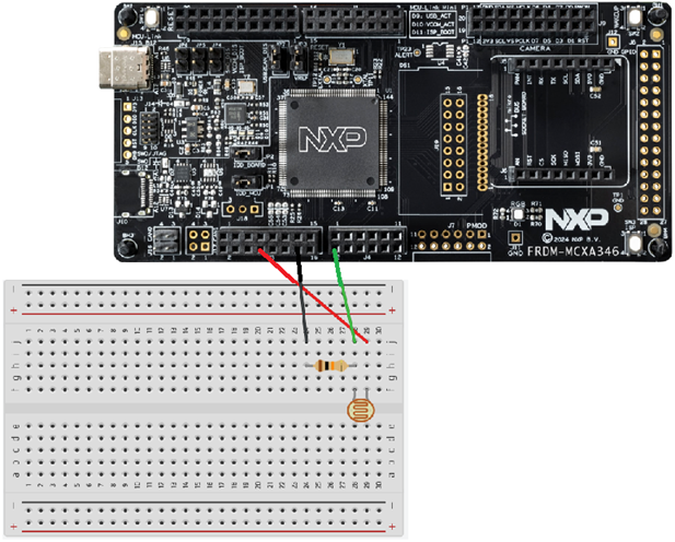
We'll use the board's LDO_3V3 pin as the voltage source in this project. Make sure to use the correct pin. Check the Quick Start Guide leaflet which came with the board to ensure you are using the correct pin. Connect a jumper wire from the same rail as the one of the second leg of the LDR and the first leg of the 10 kΩ resistor to pin P1_14 (which we configured as the ADR input pin). Connect the rail of the second leg of the resistor a GND pin.
Conclusion
You have learned how an ADC FIFO works. You now know it is a piece of hardware memory within the LPADC peripheral itself.
You've also taken your first steps in reading the Reference Manual from a hardware-centric perspective and learned how to connect specific hardware concepts - such as FCTRL, FCOUNT, FWMARK, RDY, and IE - to the corresponding SDK structures and driver functions.
As you gain more experience, this ability to translate hardware descriptions into software behavior allows you to reason about the system from the silicon upward, which may often be the key to solving subtle bugs or designing robust real-time behavior.
In a future article, I will explore DMA (Direct Memory Access). DMA offloads data movement from the CPU, reducing latency and improving real-time determinism - an important next step in building efficient embedded architectures.